- 您现在的位置:买卖IC网 > Sheet目录484 > NOIL2SC1300A-GDC (ON Semiconductor)IC IMAGE SENSOR LUPA1300 168PGA
NOIL2SM1300A
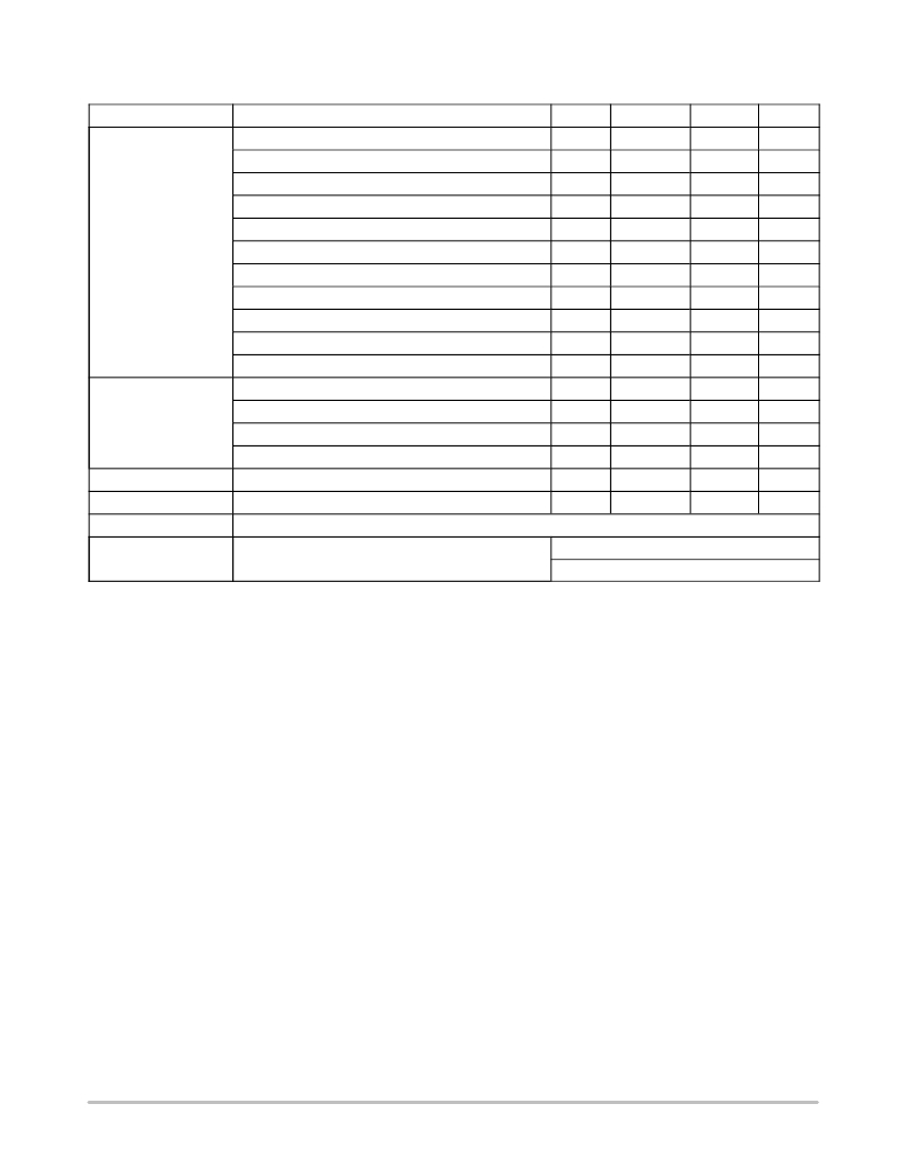
Table 22. MECHANICAL SPECIFICATIONS
Parameter
Die
(Pin 1 is located
bottom left)
Glass Lid
Mechanical Shock
Vibration
Description
Die thickness
Die position, X offset to the package center
Die position, Y offset to the package center
Die position, X tilt
Die position, Y tilt
Die placement accuracy in package
Die rotation accuracy
Optical center referenced from the die center (X-dir)
Optical center referenced from the die center (Y-dir)
Distance from PCB plane to top of the die surface
Distance from top of the die surface to top of the glass lid
XY size
Thickness
Spectral range for optical coating of window
Reflection coefficient for window (refer to Figure 36)
JESD22-B104C; Condition G
JESD22-B103B; Condition 1
Min
NA
NA
NA
-1
-1
-50
-1
NA
NA
NA
NA
NA
NA
400
NA
NA
20
Typ
750
-42
-150
0
0
0
0
-121
+2280
1.75
1.15
27.4 x 27.4
0.9
-
<0.8
2000
-
Max
NA
NA
NA
1
1
50
1
NA
NA
NA
NA
NA
NA
1100
NA
NA
2000
Units
m m
m m
m m
deg
deg
m m
deg
m m
m m
mm
mm
mm
mm
nm
%
G
Hz
Mounting Profile
Pb-free wave soldering profile for pin grid array package if no socket is used
Recommended Socket
Manufacturer
Andon Electronics (www.andonelectronics.com)
http://onsemi.com
40
BGA Socket: 10-24-05-168-319T-P27-L14
Thru Hole: 10-24-05-168-347T-P27-L14
发布紧急采购,3分钟左右您将得到回复。
相关PDF资料
NOIV1SE025KA-GDC
IC IMAGE SENSOR 25MP 355PGA
NP100P04PDG-E1-AY
MOSFET P-CH -40V MP-25ZP/TO-263
NP100P04PLG-E1-AY
MOSFET P-CH -40V MP-25ZP/TO-263
NP100P06PDG-E1-AY
MOSFET P-CH -60V MP-25ZP/TO-263
NP100P06PLG-E1-AY
MOSFET P-CH -60V MP-25ZP/TO-263
NP109N04PUJ-E1B-AY
MOSFET N-CH 40V MP-25ZP/TO-263
NP109N055PUJ-E1B-AY
MOSFET N-CH 55V MP-25ZP/TO-263
NP110N03PUG-E1-AY
MOSFET N-CH 30V MP-25ZP/TO-263
相关代理商/技术参数
NOIL2SM1300A-GDC
功能描述:IC IMAGE SENSOR LUPA1300 168PGA RoHS:是 类别:传感器,转换器 >> 图像,相机 系列:* 标准包装:480 系列:- 象素大小:6.7µm x 6.7µm 有源象素阵列:768H x 488V 每秒帧数:52 电源电压:3.3V 类型:CMOS 成像 封装/外壳:48-QFP 供应商设备封装:48-QFP 包装:托盘 请注意:* 配用:4H2105-ND - HEADBOARD FOR KAC-004014H2104-ND - KIT EVAL FOR KAC-00401 其它名称:4H20954H2095-NDKAC-00401-CBC-LB-A0
NOIL2SM1300A-GWC
功能描述:IC IMAGE SENSOR LUPA1300 168PGA RoHS:是 类别:传感器,转换器 >> 图像,相机 系列:* 标准包装:480 系列:- 象素大小:6.7µm x 6.7µm 有源象素阵列:768H x 488V 每秒帧数:52 电源电压:3.3V 类型:CMOS 成像 封装/外壳:48-QFP 供应商设备封装:48-QFP 包装:托盘 请注意:* 配用:4H2105-ND - HEADBOARD FOR KAC-004014H2104-ND - KIT EVAL FOR KAC-00401 其它名称:4H20954H2095-NDKAC-00401-CBC-LB-A0
NOIS1SC1000A-HHC
制造商:ON Semiconductor 功能描述:STAR1000 COLOR JLCC84 - Trays 制造商:ON Semiconductor 功能描述:IC IMAGE SENSOR STAR1000 84JLCC
NOIS1SM0250A-HHC
制造商:ON Semiconductor 功能描述:STAR250 JLCC84 - Trays 制造商:ON Semiconductor 功能描述:IC IMAGE SENSOR STAR250 84JLCC
NOIS1SM0250A-WWC
制造商:ON Semiconductor 功能描述:STAR250 WAFER SALES - Waffle Pack
NOIS1SM0250S-HHC
制造商:ON Semiconductor 功能描述:STAR250 JLCC84 SPACE - Trays 制造商:ON Semiconductor 功能描述:IC IMAGE SENSOR STAR250 84JLCC
NOIS1SM1000A-HHC
制造商:ON Semiconductor 功能描述:Image Sensor Monochrome CMOS 1024x1024Pixels 84-Pin JLCC Tray 制造商:ON Semiconductor 功能描述:STAR1000 JLCC84 - Trays 制造商:ON Semiconductor 功能描述:IC IMAGE SENSOR STAR1000 84JLCC
NOIS1SM1000S-HHC
制造商:ON Semiconductor 功能描述:Image Sensor Monochrome CMOS 1024x1024Pixels 84-Pin JLCC Tray 制造商:ON Semiconductor 功能描述:STAR1000 JLCC84 SPACE - Trays 制造商:ON Semiconductor 功能描述:IC IMAGE SENSOR STAR1000 84JLCC
